Full Adder Circuit Diagram: A Complete Tutorial
Know it All about Full Adder Circuit Diagram
In the electronics and the digital logic design world, the adder, in actuality, is a digital circuit used to perform addition on binary numbers. The adders are used to perform the Arithmetic Logic Unit(ALU) task in the processors when it comes to the computers. In processors, they are used to calculate addresses, increment or decrement operations, table indices, and other operations.
Source: www.elprocus.com
They are also used for number representations like binary-coded decimal code or excess-3. There are two kinds of adders.
Before jumping into the full adder, it is necessary to know what is the half adder because it is the basis of the full adder.
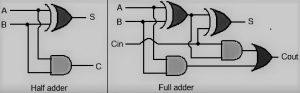
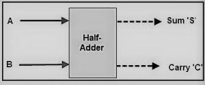
Half adder is also a circuit used in electronics and digital logic design operations. It is also used to perform addition on binary numbers. In the half adder circuit, we have two single-bit binary digits, 0 or 1, and they are the two inputs A and B of the circuit. These inputs are also called the augend and addend bits. These inputs are added, and the Sum S with the carry C is produced.
The two-half adder can be merged to form a full adder circuit. This is the simple definition of the half adder. Now, let’s dive into the full adder.
Source: www.elprocus.com
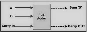
A full adder is used when you have one or more than the one-bit binary numbers. It is also a circuit used in electronics and digital logic design and is used to perform addition on the two binary inputs. The full adder inputs are three, and they are the A, B, the two standard inputs, and the Carry C, which makes it different from the half adder circuit.
In the full adder, the first carry C is always zero when the first add operation starts. When the Sum S is generated from A and B, the carry from the last least significant bit is added to the next to add operation, and this task is continued till all the binary numbers are added.
The full adder also adds 8, 16, 32, etc. bits binary numbers, which is why it is the component in the cascade of adders. The full adder usually produces a two-bit binary number as the output. If doing the summary of the full adder, they can be represented in the equations.
Source: www.elprocus.com

・ Simple alternative to Visio
・ 26k+ symbols
・ 10K+ free templates
・ 10+ AI diagram generators
Studying theory is not enough. We have also had to see the practical implementations so that our concepts become more apparent. This section will practically implement the full adder circuit diagram, truth table, and equation. And will know the process of making a full adder in three ways.
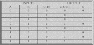
The full adder is a little complex to implement as compared to the half adder because the full adder has three inputs A, B, and C. Usually, the output is C, and the Sum S. Let’s understand the full adder from its truth table.
Source: www.elprocus.com
So, here we have two make two broad sections for input operations and output results. In the input section, we have three columns for A, B, and Cin. Now in A and B, put the 0s and 1s in the traditional form. First, take the 0s and 1s of A and B and XOR them together. When the number of 1s in input is odd in the XOR operation, the 1 is produced in the result, else 0.
Now, take the XORed A and B results and again XOR it with Cin. Remember, the first Cin is always 0. In the output section, Cout and S are generated by seeing the three inputs. If the highs(1) are odd, then the high(1) is produced as 0. Now, we will see the circuit diagram of the full adder.
Source: www.elprocus.com
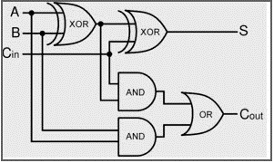
This is the general circuit diagram representation of the Full Adder. Here, we have used two half-adder diagrams to make the full adder diagram. The two inputs A and B, are first XORed, and from their result, the C is also XORed.
The inputs A and B then ANDed and then XORed A and B and Cin are also ANDed together. Both ANDs result is Ored together to produce the final Cout.
So, from the above diagram, we can easily understand that the full adder is the combinational circuit. Now, let’s see the equation or expression of the full adder circuit.
The equation or expression of the full adder is are, and they are as follows.
From the above equation of the sum S, it is easily visible that first A and B are XORed together, then Cin. ⊕ is the symbol of the XOR operation. In the Cout expression, we can see that first A and B are ANDed together, and then the Cin is ANDed with the XORed for A and B. Then, these results are ORed together to produce the Cout equation.
So, from the above working, we can say that in the full adder, three logic gates are used, and they are.
The useful electronic machines we are seeing and using today are due to the adder’s mercy. As seen above, the full adder is used to perform the Arithmetic Logic Unit Operations, a necessary part of the computer CPU operations. Without this, we will not be able to perform any complex work that computers are doing today. The full adders are used to program the chips, and these chips are used in modern vehicles, planes, and other automatic machinery. So, we can’t ignore the full adder from our life.
For this complex design of circuits using full adders, experts recommend using the best software on the internet, EdrawMax. EdrawMax is an easy-to-use diagram-making software that you can use to perform your task efficiently.
The developers of the software say that the software is for everyone regardless of their professional background. The software contains all the essential pre-generated templates and libraries that you use to boost your production. You can also download your result in different formats and share them on any social media site. The software is free for your primary work, but you have to purchase the software if you want more advanced features.